- 您现在的位置:买卖IC网 > Sheet目录17359 > ADR4533BRZ (Analog Devices Inc)IC VREF SERIES PREC 3.3V 8SOIC
ADR4520/ADR4525/ADR4530/ADR4533/ADR4540/ADR4550
ADR4525
Data Sheet
2.5005
ADR4525
1.4
ADR4525
2.5004
2.5003
2.5002
2.5001
1.2
1.0
0.8
+125°C
–40°C
+25°C
2.5000
2.4999
2.4998
0.6
0.4
2.4997
0.2
2.4996
2.4995
0
–50
–30
–10
10
30
50
70
90
110
130
–15
–10
–5
0
5
10
15
TEMPERATURE (°C)
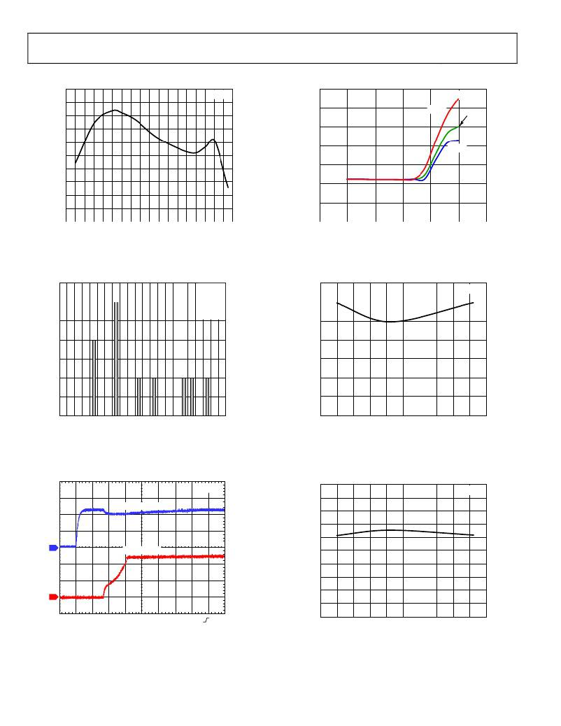
Figure 18. ADR4525 Output Voltage vs. Temperature
I LOAD (mA)
Figure 21. ADR4525 Dropout Voltage vs. Load Current
3.5
3.0
ADR4520
ADR4525
ADR4530
ADR4533
35
30
ADR4525
ADR4540
ADR4550
2.5
2.0
1.5
1.0
0.5
25
20
15
10
5
0
0
–60
–40
–20
0
20
40
60
80
100
120
140
TEMPERATURE (°C)
ΔV OUT_HYS (ppm)
Figure 19. ADR4525 Thermally Induced Output Voltage Hysteresis Distribution
Figure 22. ADR4525 Load Regulation vs. Temperature (Sourcing)
V IN (5V/DIV)
ADR4525
100
90
80
70
60
ADR4525
1
V OUT (1V/DIV)
50
40
30
20
2
10
CH1 5.00V
CH2 1.00V
M40.0μs
A CH1
9.10V
0
–60
–40
–20
0
20
40
60
80
100
120
140
TEMPERATURE (°C)
Figure 20. ADR4525 Output Voltage Start-Up Response
Rev. 0 | Page 14 of 32
Figure 23. ADR4525 Load Regulation vs. Temperature (Sinking)
发布紧急采购,3分钟左右您将得到回复。
相关PDF资料
A9BBA-0203F
FLEX CABLE - AFF02A/AF02/AFF02A
ADR4520BRZ
IC VREF SERIES PREC 2.048V 8SOIC
RBC06DRTI
CONN EDGECARD 12POS DIP .100 SLD
A9BAG-0603F
FLEX CABLE - AFF06G/AF06/AFE06T
MIC2546-1BM
IC SW CURR LIMIT DUAL 16-SOP
ADR430ARZ
IC VREF SERIES PREC 2.048V 8SOIC
RB-2424S/H
CONV DC/DC 1W 24VIN 24VOUT
A9AAT-1706E
FLEX CABLE - AFH17T/AE17/AFH17T
相关代理商/技术参数
ADR4533BRZ_PROMO
制造商:Analog Devices 功能描述:IC V REF 15VIN 3.3V +/-0.0
ADR4533BRZ-R7
功能描述:IC VREF SERIES PREC 3.3V 8SOIC RoHS:是 类别:集成电路 (IC) >> PMIC - 电压基准 系列:- 标准包装:2,000 系列:- 基准类型:旁路,可调节,精度 输出电压:1.24 V ~ 16 V 容差:±0.5% 温度系数:- 输入电压:1.24 V ~ 16 V 通道数:1 电流 - 阴极:100µA 电流 - 静态:- 电流 - 输出:20mA 工作温度:-40°C ~ 85°C 安装类型:通孔 封装/外壳:TO-226-3、TO-92-3(TO-226AA)成形引线 供应商设备封装:TO-92-3 包装:带卷 (TR)
ADR4540
制造商:AD 制造商全称:Analog Devices 功能描述:Ultralow Noise, High Accuracy
ADR4540ARZ
功能描述:IC VREF SERIES PREC 4.096V 8SOIC RoHS:是 类别:集成电路 (IC) >> PMIC - 电压基准 系列:- 标准包装:1,000 系列:- 基准类型:旁路,可调节,精度 输出电压:2.495 V ~ 36 V 容差:±0.5% 温度系数:标准值 34ppm/°C 输入电压:2.495 V ~ 36 V 通道数:1 电流 - 阴极:1mA 电流 - 静态:- 电流 - 输出:100mA 工作温度:0°C ~ 70°C 安装类型:表面贴装 封装/外壳:TO-243AA 供应商设备封装:SOT-89-3 包装:带卷 (TR)
ADR4540ARZ_PROMO
制造商:Analog Devices 功能描述:V REF 15VIN 4.096V +/-0.04%
ADR4540ARZ-R7
功能描述:IC VREF SERIES PREC 4.096V 8SOIC RoHS:是 类别:集成电路 (IC) >> PMIC - 电压基准 系列:- 产品培训模块:Voltage Reference Basics 标准包装:100 系列:- 基准类型:旁路,精度 输出电压:4.096V 容差:±0.075% 温度系数:50ppm/°C 输入电压:- 通道数:1 电流 - 阴极:1µA 电流 - 静态:- 电流 - 输出:10mA 工作温度:0°C ~ 70°C 安装类型:表面贴装 封装/外壳:8-SOIC(0.154",3.90mm 宽) 供应商设备封装:8-SOIC 包装:管件
ADR4540BRZ
功能描述:IC VREF SERIES PREC 4.096V 8SOIC RoHS:是 类别:集成电路 (IC) >> PMIC - 电压基准 系列:- 标准包装:1,000 系列:- 基准类型:旁路,可调节,精度 输出电压:2.495 V ~ 36 V 容差:±0.5% 温度系数:标准值 34ppm/°C 输入电压:2.495 V ~ 36 V 通道数:1 电流 - 阴极:1mA 电流 - 静态:- 电流 - 输出:100mA 工作温度:0°C ~ 70°C 安装类型:表面贴装 封装/外壳:TO-243AA 供应商设备封装:SOT-89-3 包装:带卷 (TR)
ADR4540BRZ_PROMO
制造商:Analog Devices 功能描述:V REF 15VIN 4.096V +/-0.02%
